 Ceramic parts are made from inorganic, non-metallic materials and provide high functionality for components in equipment and devices with diverse functions. With their crystalline, partly crystalline, and amorphous glass structure, engineered ceramics have solved numerus problems in electrical, chemical, and mechanical applications.
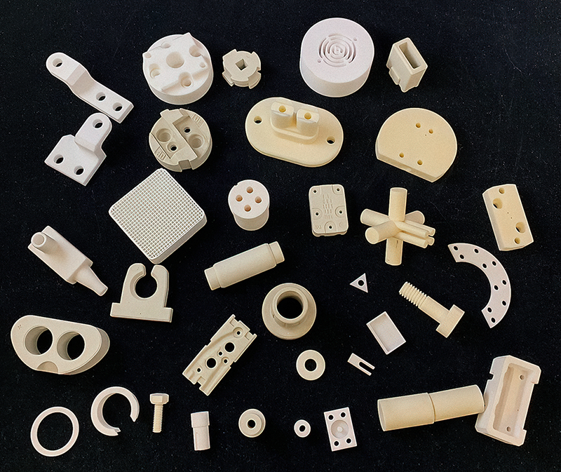
The high heat resistance of ceramics enables them function when metal and polymers are unsuitable. Ceramics composition can be tailored for suitability for use in both active (carrying electric signal) and passive parts, and can be manufactured into a multitude of shapes and sizes with green machining, lapping, drilling, sintering, laser machining, and polishing. Our ceramics can be metalized and brazed to your specifications.
Fralock’s ceramics encompass a wide range of thermal conductivities. Aluminum Nitride (AlN) heaters reach up to 180W/mK, heaters made with alumina are capable of 15 W/mK to 20 W/mK, and zirconia-based heating products achieve 2.7 W/mK. High thermally conductive ceramics may also be used as heat spreaders with dielectric capabilities. Lower thermal conductive materials can be used as thermal breaks or insulators, and can be coupled with high thermally conductive AlN heaters. Depending on your needs, you can count on us to utilize optimal materials for your requirements.
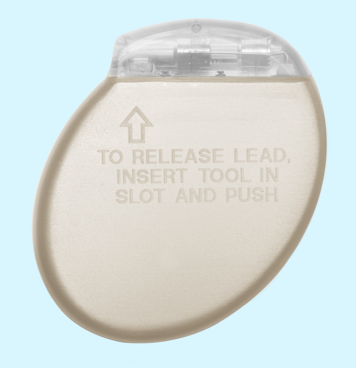
Engineered ceramics are used in a wide range of industries including semiconductor manufacturing, medicine and life science, aerospace, military defense, electronics, industrial and transmission electricity, and energy production.
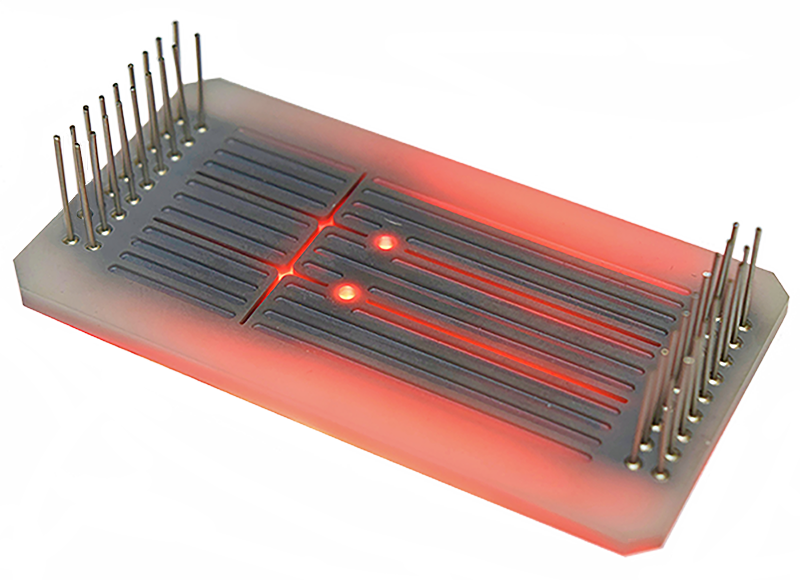
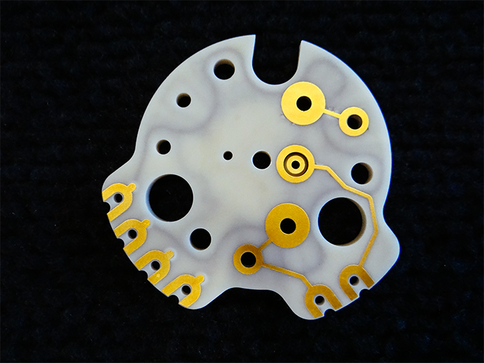
 Layered Ceramic Heaters – Using a unique formulation of Aluminum Nitride ceramic with co-fired internal Tungsten (W) traces for heating and temperature sensing, we design and manufacture rapid-fire heaters with exceptional thermal uniformity, watt density, and temperature ramping capabilities for use in semiconductor wafer fabrication, aerospace and defense, and medical applications. With rapid heating up to 300ºC/second, this laminated material can be configured in many shapes and sizes and precision-machined with air or fluid channels that enhance cooling.
Stainless Steel and Borosilicate Glass Heaters – Formulated with a Borosilicate glass dielectric layer, these heaters enable high temperature generation and robust electrical functionality for lower costs.
Applications: High-temperature heaters that require extremely rapid thermal cycling with thermal uniformity, may require multiple heating zones, and/or sensor-feedback temperature control is required.